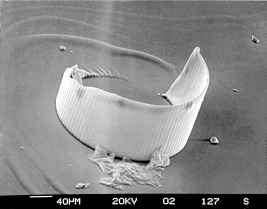
 figure at left
shows a 3-D object written into a commercial photoresist using
2-photon absorption. The object was made by translating the
substrate along the focus of the beam while simultaneously rotating it
in the plane normal to the beam. The "fluted" appearance results
from columns of exposed resist, each created by the exposure of a
single laser shot; the optical set-up used here produces roughly
cylindrical columns with a ~4 µm diameter and a ~75 µm
height. The short columns at left are produced when most of the
focal volume is in the substrate below the plane of the
photoresist. As the sample translates into the beam focus, the
focal volume moves into the resist layer, creating a series of adjacent
columns of progressively increasing height. On the right side of
the figure, the sample has translated so that the full column height is
in the center of the resist layer and is not anchored to the
substrate. The region under these columns was undercut when
the resist was etched, resulting in a local collapse of the structure
(this is why the structure is a partial ring instead of a spiral
ribbon). There are roughly 80 columns in the structure; since the
laser has a 1 kHz repetition rate, the entire structure was written in
80 msec. In addition to writing 3-D structures in
conventional photoresist, we also have shown that multiphoton
absorption can be used to expose commercial photographic film.
We also have developed the 3-D equivalent of photography by "writing"
3-D patterns of Ag nanocystals in the interior of a silica gel, a
technique with the potential for the direct 3-D lithographic production
of metal wires and circuits. Finally, in collaboration with Xiang Zhang's group
in the UCLA Dept. of Mechanical Engineering, we also have developed a
new way to write sub-diffraction-limited size features in commercial
photoresist by amplifying the intensity of the two-photon field in the
presence of a small metallic AFM tip (apertureless near-field); by
tracing the AFM tip over the sample, we have been able to write
features as small as 70 nm. We are also working to extend
our 3-D lithography techniques to molecularly imprintable polymers
that can be used as chemical sensors. See, e.g.,
P. G. Conrad II, P. T. Nishimura, D. Aherne, B. J. Schwartz, D. Wu, N. Fang, X. Zhang, J. Roberts, and K. J. Shea, “Functional Molecularly Imprinted Polymer Microstructures Fabricated Using Microstereolithographic Techniques,” Adv. Mat. 15(18), 1541-4 (2003).
X. Yin, N. Fang, X. Zhang, I. B. Martini and B. J. Schwartz, "Near-Field Two-Photon Nanolithography Using an Apertureless Optical Probe," Appl. Phys. Lett. 81(19), 3663-5 (2002).
P.-W. Wu, W. Cheng, I. B. Martini, B. Dunn, B. J. Schwartz and E. Yablonovitch, "Two-Photon Photographic Production of Three-Dimensional Metallic Structures within a Dielectric Matrix," Adv. Mat. 12(19), 1438-41 (2000).
P.-W. Wu, B. Dunn, V. Doan, B. J. Schwartz, E. Yablonovitch and M. Yamane, "Controlling the Spontaneous Precipitation of Silver Nanoparticles in Sol-Gel Matrices," J. Sol-Gel Sci. Tech. 19(1-3), 249-52 (2000).
P.-W. Wu, B. Dunn, E. Yablonovitch, V. Doan, and B. J. Schwartz, "Two-Photon Exposure of Photographic Film," J. Opt. Soc. Am. B—Opt. Phys. 16(4), 605-8 (1998).
G. Witzgall, R. Vrijen, E. Yablonovitch, V. Doan and B. J. Schwartz, "Single-Shot, Two-Photon Exposure of Commercial Photoresist for the Production of Three-Dimensional Structures," Opt. Lett. 23(22), 1745-7 (1998).